


[Reading level: B2 – Upper Intermediate]
A microchip can take up to 26 weeks to make. In its as many as 100 layers, billions of transistors are packed into an area about the size of a fingernail. They’re the brains behind almost everything we use in our increasingly electronic world. Here’s how these complex tiny devices are made.

The process begins with silicon-rich sand. Why silicon? Silicon is a semiconductor. It’s the sweet spot between an insulator and a pure conductor. That means its properties such as its conductivity can be altered by adding impurities or doping to meet the needs of different electronic devices. This also allows us to control the electrical signals that pass through.
Silicon is also abundant. It’s one of the 10 most common elements found on earth. But much of the silicon found in the wild is chemically bound to oxygen so the two elements must be separated.
The sand is combined with carbon and melted in crucibles to produce carbon monoxide and 99%-pure silicon. After further processing, ultrapure silicon is produced. Next, a seed crystal is placed in contact with molten silicon. As the seed crystal is slowly pulled away, silicon atoms are deposited on the bottom surface. The result is a large cylindrical bull or a single crystal ingot of pure silicon.
The bull is then thinly sliced into wafers. Silicon wafers typically have diameters of 1 to 12 inches with the most state-of-the-art facilities being able to produce wafers up to 18 inches in diameter. Bigger wafers are of course able to yield more microchips.
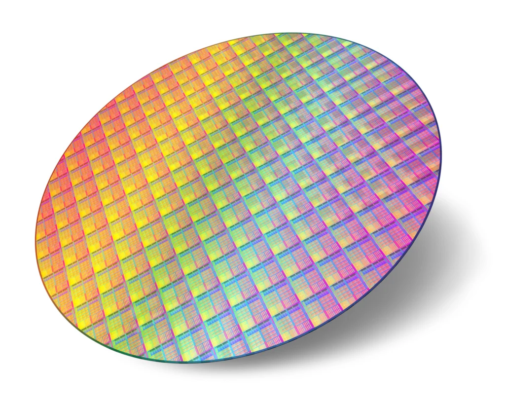
Once the silicon wafers are cut, the production process begins in full. Microchips are made in extremely sterile conditions, free from contaminants such as dust. If even just one particle of dust makes its way onto a silicon wafer, the entire batch is at risk of being ruined. This would derail a process that can take an average of 12 weeks.
The first step of the production process is deposition. A thin non-conducting layer of silicon dioxide is grown or deposited on the surface of the wafer. Then, the silicon wafer is prepared for lithography, by coating it with photosensitive and light resistant materials.

The next step is very critical: exposure. The prepared silicon wafers enter a lithography machine and are exposed to UV light passed through a reticle, containing the chip’s blueprint. The areas exposed to light are hardened while unexposed areas are then etched away by hot gases to leave a three-dimensional microchip.
The electrical conductivity of different parts of the chip can also be altered by doping them with chemicals under heat and pressure. This process can be repeated hundreds of times for the same chip, producing a more complex integrated circuit at each step.
To create conducting paths between the components, a thin layer of metal such as aluminum is overlaid onto the chip, and the etching process is used to remove everything except the thin conducting pathways. Several layers of conductors separated by glass insulators can be laid down.
Each chip on the wafer is then tested for performance before it’s separated from other chips on the wafer by a saw. Since microchips are essentially circuits built on an incredibly small scale, they have a basic set of components.
Capacitors can temporarily store an electrical charge. Resistors help control the electrical current. Transistors can either amplify or switch the electrical signals passing through.
For more advanced chips, like those found on high-end graphics cards, there can be upwards of 28 billion transistors on board.
More transistors on microchips allow them to send out more instructions, increasing the computational power. Moore’s law predicts that computer chip manufacturing would advance at a steady rate, allowing transistor counts to double every two years. Based on the sheer power of the technology we use on a day-to-day basis, this decade’s old prediction seems to still be mostly true.
Manufacturers have been shrinking down their transistor sizes to fit more onto chips. Each breakthrough in transistor size has allowed the production of more powerful chips for our phones, computers and gaming consoles.
In recent years, they’ve gotten each transistor down to as small as 8x ten to the power of negative eight inches in diameter, allowing an amazing 50 billion transistors to be crammed onto a single chip.
Manufacturing microchips is truly one of our most complex feats and yet innovations are happening every day.
Source: Interesting Engineering
WORD BANK:
microchip /ˈmaɪ.kroʊˌtʃɪp/ (n): vi mạch
transistor /trænˈzɪs.tɚ/ (n): bóng bán dẫn
fingernail /ˈfɪŋ.ɡɚ.neɪl/ (n): móng tay
complex /ˈkɑːm.pleks/ [B2] (adj): phức tạp
tiny /ˈtaɪ.ni/ [B1] (adj): rất nhỏ
silicon-rich /ˈsɪl.ɪ.kən rɪtʃ/ (adj): giàu silicon
semiconductor /ˌsem.i.kənˈdʌk.tɚ/ (n): chất bán dẫn
sweet spot /ˈswiːt spɑːt/ (n): điểm tối ưu
insulator /ˈɪn.sə.leɪ.tɚ/ (n): chất cách điện
conductor /kənˈdʌk.tɚ/ (n): chất dẫn điện
property /ˈprɑː.pɚ.t̬i/ (n): đặc tính
alter /ˈɑːl.tɚ/ [B2] (v): thay đổi
impurity /ɪmˈpjʊr.ə.t̬i/ (n): tạp chất
doping /ˈdoʊ.pɪŋ/ (n): pha tạp
pass through /pæs θruː/ (v): đi xuyên qua
abundant /əˈbʌn.dənt/ [C1] (adj): dồi dào
element /ˈel.ə.mənt/ [B1] (n): nguyên tố
chemically bound to sth /ˈkem.ɪ.kəl.i baʊnd/ (adj): liên kết hóa học với cái gì
melt /melt/ [B1] (v): nóng chảy
crucible /ˈkruː.sə.bəl/ (n): nồi nấu, lò nấu
ultrapure /ˌʌl.trəˈpjʊr/ (adj): siêu tinh khiết
seed crystal /siːd ˈkrɪs.təl/ (n): tinh thể mồi
in contact with sth /ɪn ˈkɑːn.tækt/ (pre): tiếp xúc với cái gì
molten /ˈmoʊl.tən/ (adj): nóng chảy (ở trạng thái lỏng)
pull /pʊl/ (v): kéo
deposit /dɪˈpɑː.zɪt/ (v): lắng đọng
deposition /ˌdep.əˈzɪʃ.ən/ (n): sự lắng đọng
cylindrical bull /səˈlɪn.drɪ.kəl bʊl/ (n): khối trụ (silicon)
ingot /ˈɪŋ.ɡət/ (n): thỏi (thường là kim loại)
wafer /ˈweɪ.fɚ/ (n): tấm wafer
diameter /daɪˈæm.ə.t̬ɚ/ [B2] (n): đường kính
state-of-the-art /ˌsteɪt.əv.ðiːˈɑːrt/ (adj): tối tân, hiện đại nhất
in full /ɪn fʊl/ (adv): đầy đủ
sterile /ˈster.əl/ (adj): vô trùng
contaminant /kənˈtæm.ə.nənt/ (n): chất gây nhiễm bẩn
particle /ˈpɑːr.t̬ə.kəl/ [B2] (n): hạt
the entire sth /ði ɪnˈtaɪr/ (det): toàn bộ cái gì
batch /bætʃ/ (n): lô, mẻ
derail sth /ˌdiːˈreɪl/ (v): làm trật hướng, làm hỏng
lithography /lɪˈθɑː.ɡrə.fi/ (n): quang khắc
coat sth with sth /koʊt/ (v): phủ cái gì bằng cái gì
photosensitive /ˌfoʊ.t̬oʊˈsen.sə.t̬ɪv/ (adj): nhạy sáng
light-resistant /ˈlaɪt rɪˌzɪs.tənt/ (adj): chống ánh sáng
exposure /ɪkˈspoʊ.ʒɚ/ [B2] (n): sự phơi sáng
reticle /ˈret̬.ɪ.kəl/ (n): mặt nạ (mask) trong quang khắc
blueprint /ˈbluː.prɪnt/ [C1] (n): bản thiết kế
harden /ˈhɑːr.dən/ [B2] (v): cứng lại
etch /etʃ/ (v): khắc, ăn mòn
etch sth away /etʃ əˈweɪ/ (v): khắc bỏ đi
three-dimensional /ˌθriː.dɪˈmen.ʃən.əl/ [C1] (adj): ba chiều
integrated circuit /ˈɪn.t̬ə.ɡreɪ.t̬ɪd ˈsɜːr.kɪt/ (n): mạch tích hợp
conducting path /kənˈdʌk.tɪŋ pæθ/ (n): đường dẫn điện
overlay /ˈoʊ.vɚ.leɪ/ (n): lớp phủ
saw /sɑː/ (n): cái cưa
capacitor /kəˈpæs.ə.t̬ɚ/ (n): tụ điện
electrical charge /ɪˈlek.trɪ.kəl tʃɑːrdʒ/ (n): điện tích
resistor /rɪˈzɪs.tɚ/ (n): điện trở
electrical current /ɪˈlek.trɪ.kəl ˈkɝː.ənt/ (n): dòng điện
amplify sth /ˈæm.plə.faɪ/ [C1] (v): khuếch đại
switch sth /swɪtʃ/ (v): chuyển đổi
high-end /ˌhaɪˈend/ (adj): cao cấp
graphics card /ˈɡræf.ɪks kɑːrd/ (n): card đồ họa
computational /ˌkɑːm.pjəˈteɪ.ʃən.əl/ (adj): tính toán
Moore’s law /mʊrz lɔː/ (n): định luật Moore
count /kaʊnt/ (v): đếm, số lượng
on a day-to-day basis /ˌdeɪ.t̬əˈdeɪ ˈbeɪ.sɪs/ (adv): hằng ngày
shrink /ʃrɪŋk/ [B2] (v): thu nhỏ
gaming console /ˈɡeɪ.mɪŋ ˌkɑːn.soʊl/ (n): máy chơi game
cram /kræm/ (v): nhồi, nhét
feat /fiːt/ (n): kỳ tích, thành tựu
ỦNG HỘ READ TO LEAD!
Chào bạn! Có thể bạn chưa biết, Read to Lead là một trang giáo dục phi lợi nhuận với mục đích góp phần phát triển cộng đồng người học tiếng Anh tại Việt Nam. Chúng tôi không yêu cầu người đọc phải trả bất kỳ chi phí nào để sử dụng các sản phẩm của mình để mọi người đều có cơ hội học tập tốt hơn. Tuy nhiên, nếu bạn có thể, chúng tôi mong nhận được sự hỗ trợ tài chính từ bạn để duy trì hoạt động của trang và phát triển các sản phẩm mới.
Bạn có thể ủng hộ chúng tôi qua 1 trong 2 cách dưới đây.
– Cách 1: Chuyển tiền qua tài khoản Momo.
Số điện thoại 0947.886.865 (Chủ tài khoản: Nguyễn Tiến Trung)
Nội dung chuyển tiền: Ủng hộ Read to Lead
hoặc
– Cách 2: Chuyển tiền qua tài khoản ngân hàng.
Ngân hàng VIB chi nhánh Hải Phòng
Số tài khoản: 012704060048394 (Chủ tài khoản: Nguyễn Tiến Trung)
Nội dung chuyển tiền: Ủng hộ Read to Lead
Lớp luyện thi IELTS online
Bạn đang có nhu cầu thi chứng chỉ IELTS cho đầu vào đại học, đi du học, xin việc hay xin cư trú và đang phân vân chưa biết học ở đâu?
Nếu bạn đang tìm kiếm dịch vụ luyện thi IELTS online với giáo viên uy tín và chất lượng, cũng như học phí phải chăng, thì thầy Trung và Cô Thủy (Admin và dịch giả chính của Read to Lead) có thể là một lựa chọn phù hợp dành cho bạn.
Hãy liên hệ (nhắn tin) tới trang Facebook cá nhân của mình (https://www.facebook.com/nguyen.trung.509) để tìm hiểu về lớp học và được tư vấn cũng như được học thử nha!

